Sigfox Base Station Reverse Engineering - Part 2: RF Power Amplifier
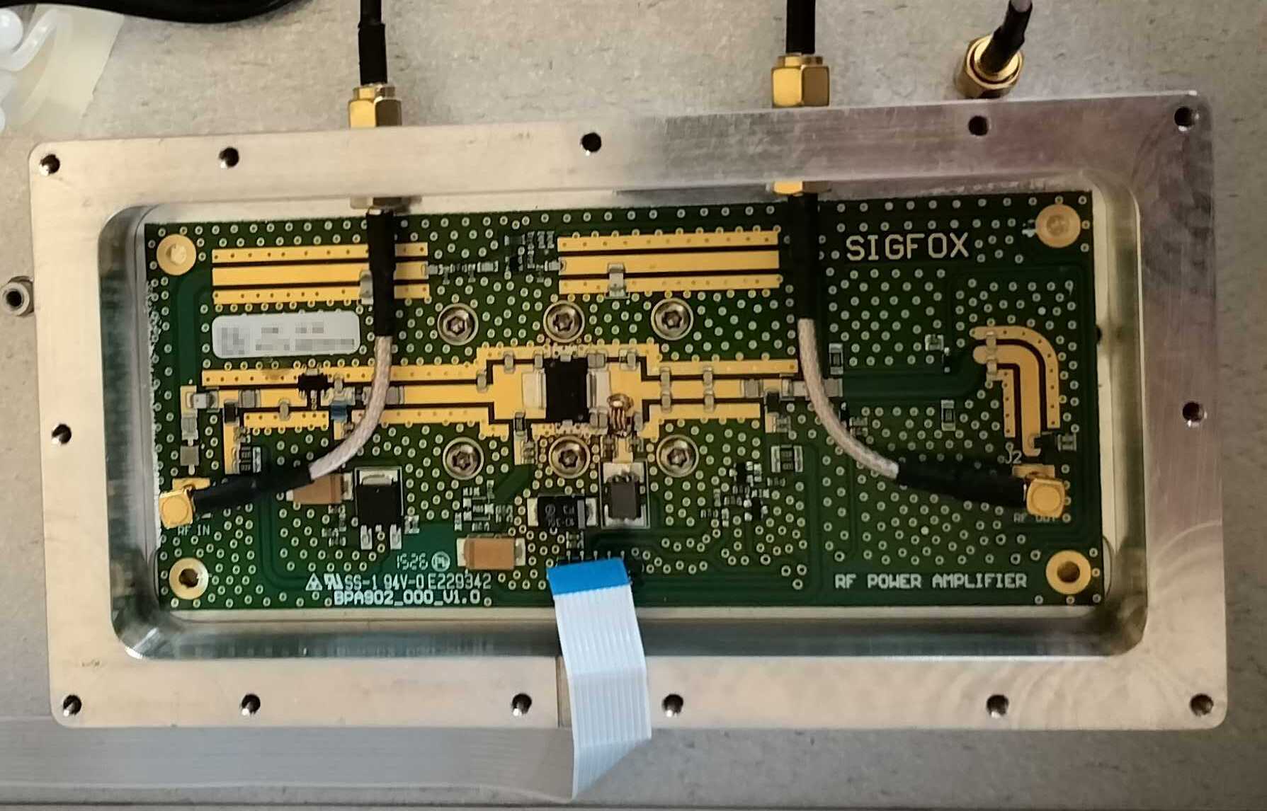
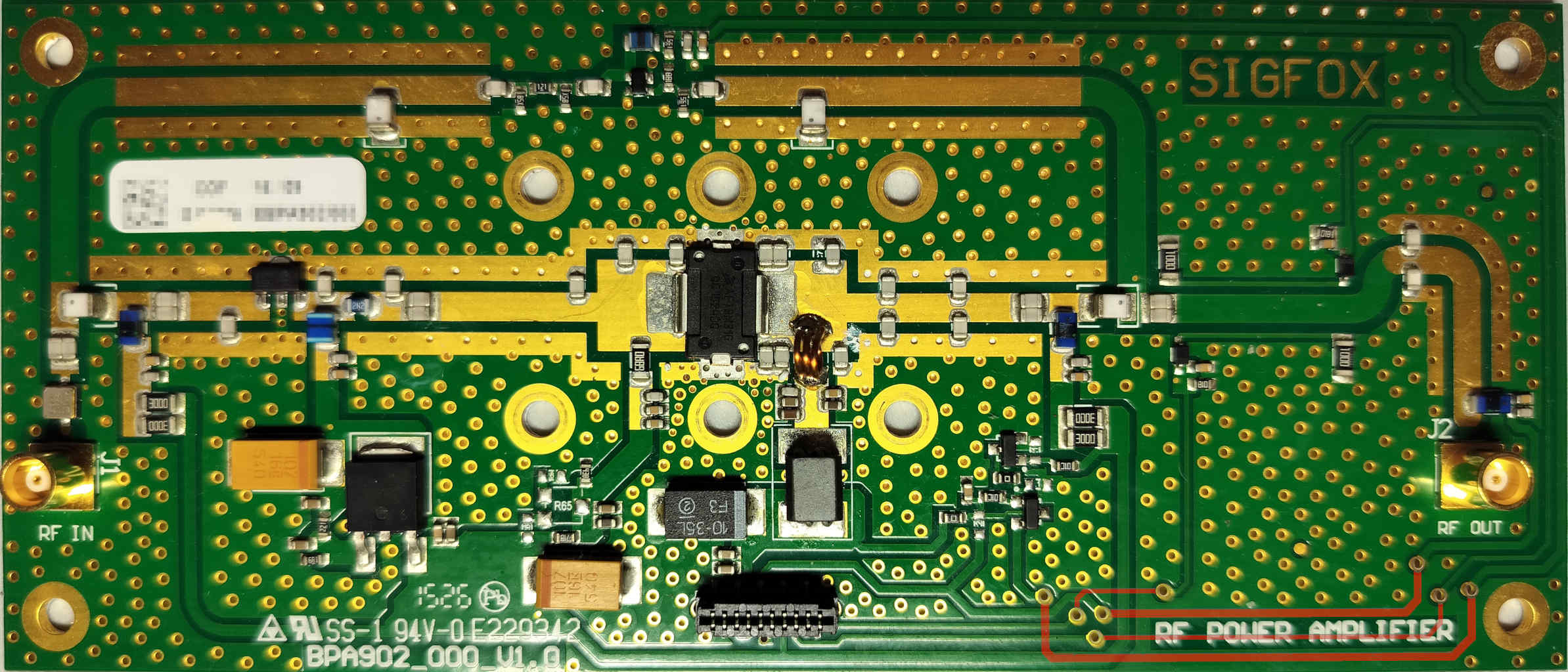
Now that I’ve given an overview of the Sigfox base station, I’ll start diving deeper into the individual components. I’ll start here with the RF Power Amplifier, denoted as BPA (Base station Power Amplifier, perhaps? But it’s also possible it could include French words as that is where Sigfox is based) on the PCB. This is the last stage outgoing signals pass through on the way out of the base station, and the first stage they pass through on the way in (ignoring the LNA that is external to the unit). This amplifier is responsible for amplifying outgoing signals to a appropriate power level, and also amplifying incoming signals to a level that the SDR can work with.
This one will be relatively brief, as the power amplifier is a fairly simple component, at least in comparison to the SDR. Additionally I should note that I am by no means an expert on RF electronics, more-or-less everything I know is self taught and I never had any formal education in that area (Computer Engineering degrees didn’t require them like Electrical Engineering did). So it is possible I mess something up in the analysis or explanations.
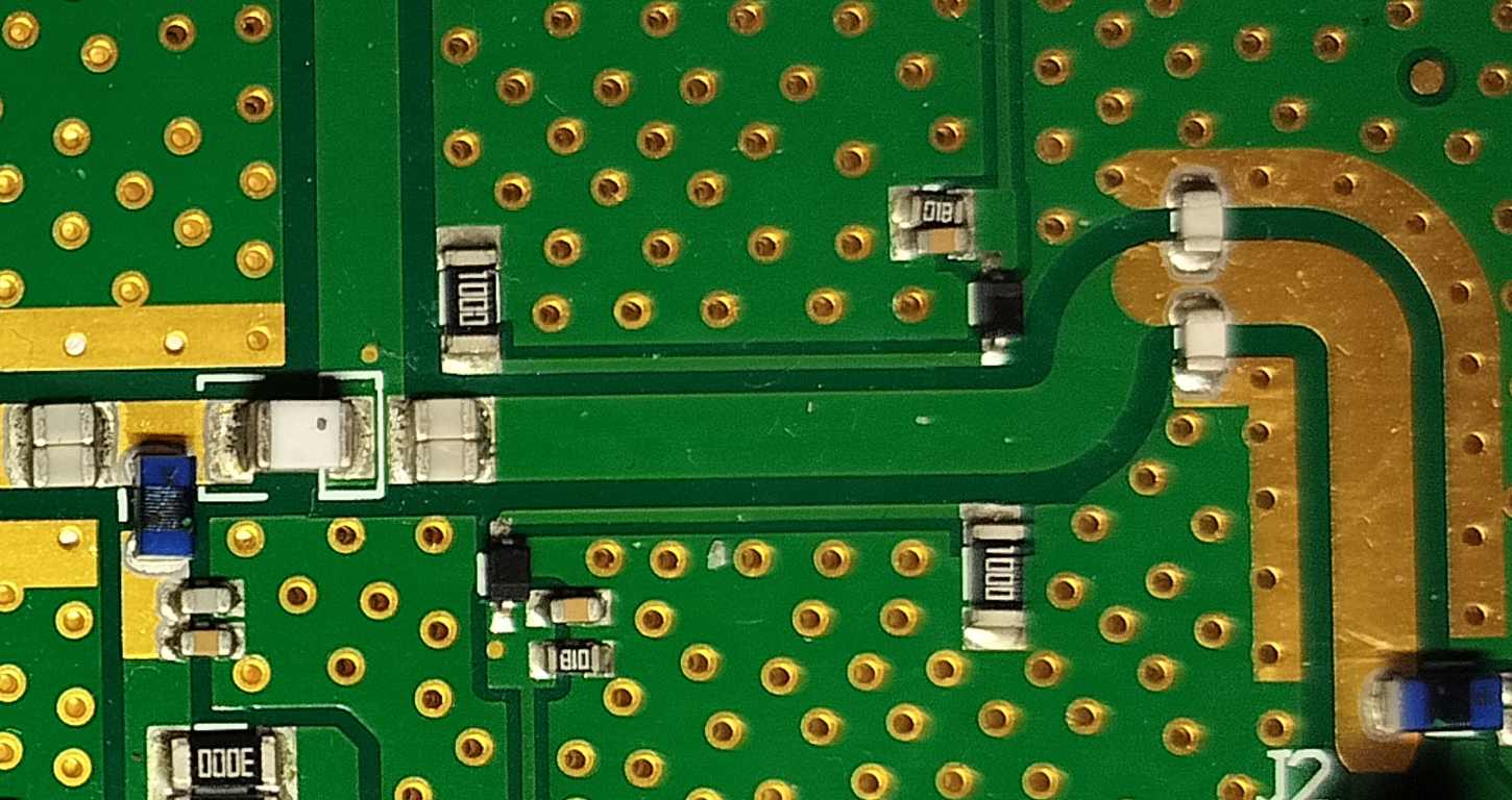
I didn’t have any particular strategy while reverse-engineering the amplifier, I just followed the path from input to output, then filled in whatever I missed. Thankfully this is only a two layer board, and with very few traces disappearing behind components. Due to the PCB only using SMD components, and having no components on the underside, I was able to get a good picture of the rear using a scanner (not that this board really needed it, since there are only a total of four traces on the rear). Much clearer than the best pictures I was able to get using my cellphone camera.
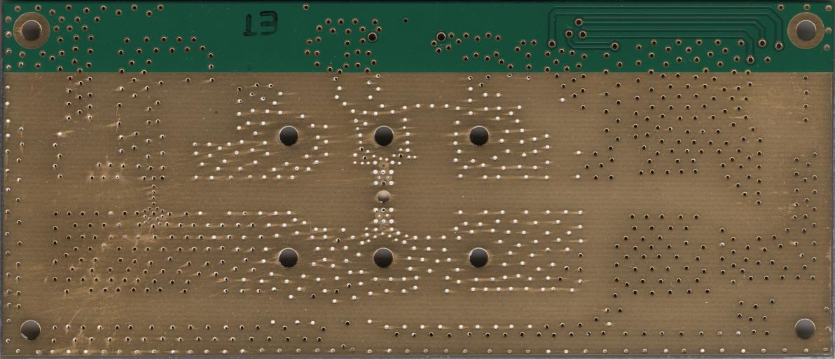
To make things slightly easier, I took the scan of the rear and deleted everything but the few traces in GIMP. Then (after changing their color to make them stand out more) I layered that on top of the picture of the top (using the perspective tool to make everything line up):
While I was going through the process of reverse-engineering the board, I simply drew out the schematic on paper. I find this much easier than trying to put it in KiCAD or other EDA tool, as it’s much easier to make changes and make notes throughout the process. (I apologize for the handwriting)
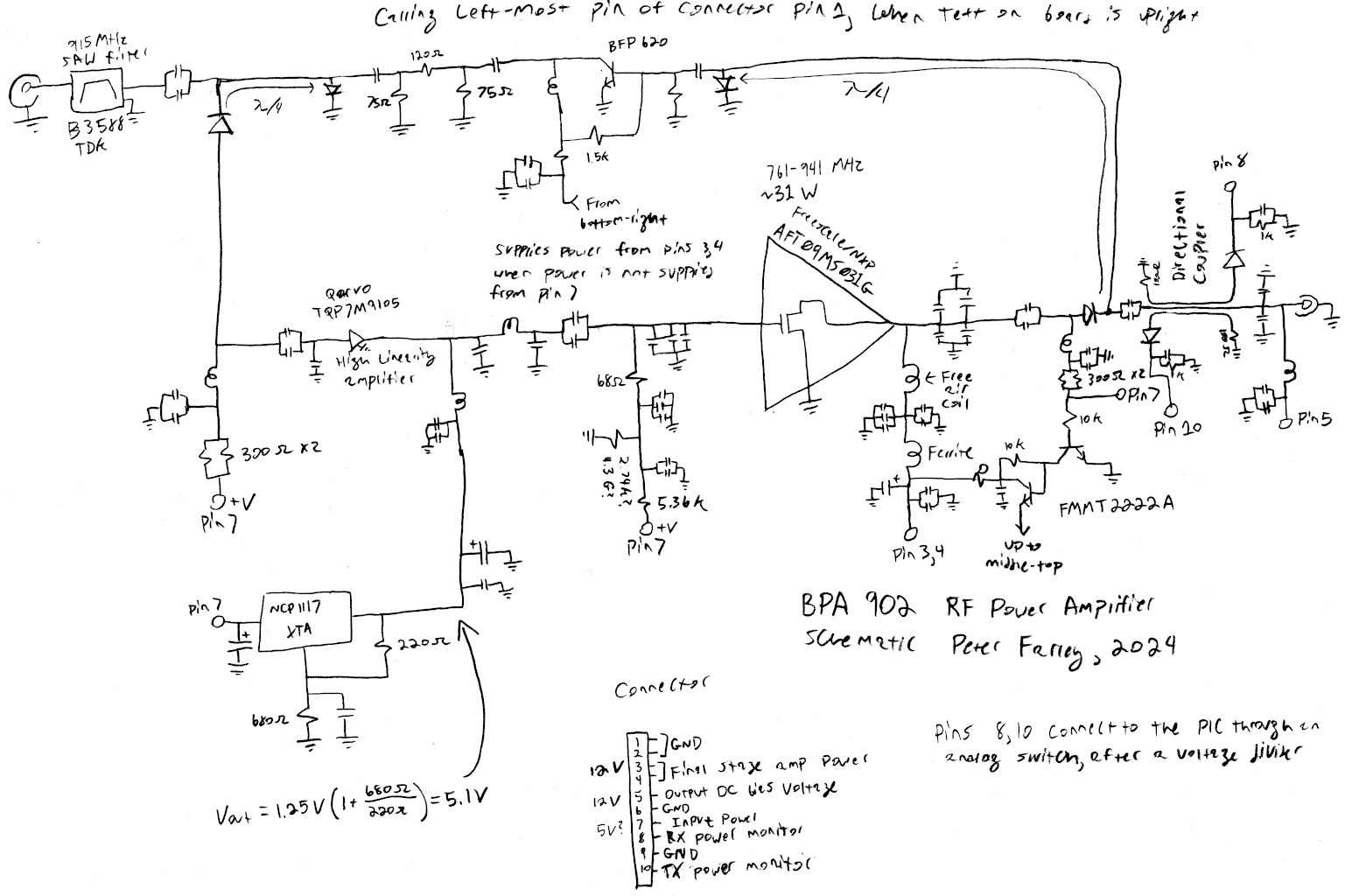
Once I had the schematic completed, I created a block diagram to simplify the RF paths:
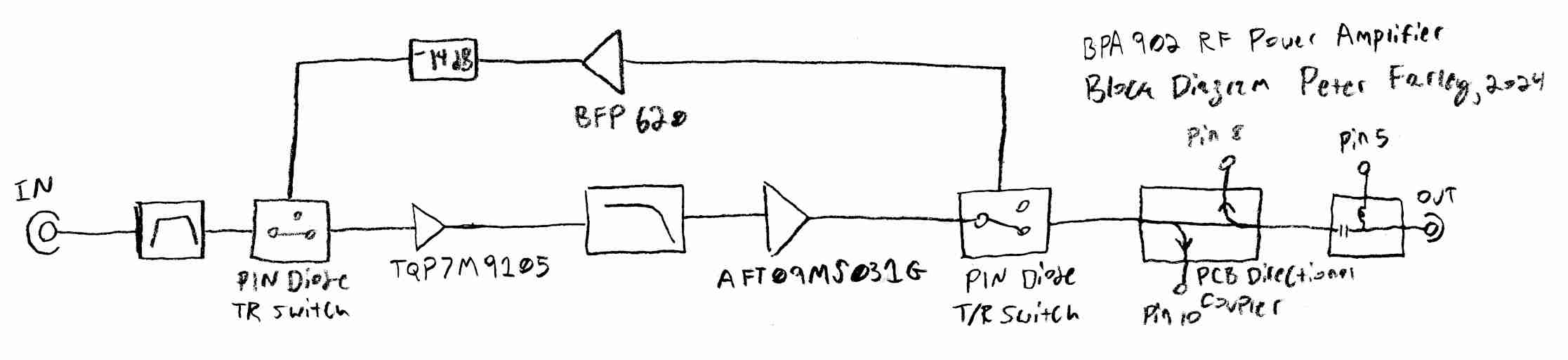
TX Path
When the signal comes in to the amp, the first thing it hits is a filter. Specifically, a Qualcomm/TDK B3588 915 MHz (~26 MHz bandwidth) SAW (Surface Acoustic Wave) filter.

(Image courtesy of “Introduction to SAW Filter Theory & Design Techniques” from apitech)
SAW filters work by converting the electrical signal into a mechanical movement and back again, using a piezoelectric material, hence the name (an acoustic wave travels on the surface of the material between the two transducers). The input and output transducers are formed by interlocking comb electrodes, the period of the teeth determining the filter’s frequency response. These transducers are called interdigital transducers, or IDTs.
What comes after the filter stumped me for a little while. At first, I had assumed that the larger white ceramic SMD components were capacitors or some other passive component, but then there would be a couple bias tees that seemed useless with capacitors on both sides. When I was removing one of them to measure it (on board it was measuring as a capacitor at some frequencies, and a resistor at others), I noticed the silkscreen underneath the part started with “D”, at which point I realized it was actually a diode. (I also accidentally flung the diode across my desk while measuring it and couldn’t find it for a day - thankfully I did, since they are around $6 a pop). Not sure why I didn’t realize that sooner, with the dot on the cathode side of the package.
Once I figured out that it was a diode (specifically a PIN diode), things made a lot more sense. The two diodes (one on the transmit path, the other on the receive path) make up a T/R (transmit/receive) switch. PIN diodes are often used for RF switches due to their low capacitance in the non-forward-biased state, and low resistance in the forward-biased state. They are also slow to switch from conduction to non conducting when switched from forward- to reverse-bias (i.e. they have a long “reverse recovery time”), meaning they can still conduct if the signal has a high enough amplitude to reverse-bias the diode at it’s minimum.
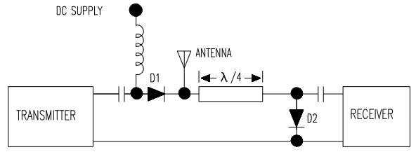
(Image courtesy of “PIN Diode Circuit Designers’ Handbook” from Microsemi)
Knowing this, it still was not immediately apparent how this switch worked. Looking at the schematic, applying a positive enough bias to enable conduction to the transmit path will also enable conduction on the shunt diode on the receive path. At first glance, this would result in a dead short, and no signal making it into the receive path. However, measuring the trace from the one PIN diode to the other (about 4~5 cm), it turns out it is about 1/4 of a wavelength of 915 MHz on copper-clad FR-4 (3.8~5.3 depending on the dielectric constant). A quarter-wave of transmission line can act as an impedance transformer, making the dead short from the diode actually appear as an open. When the bias is not applied, the transmit path is disconnected, and the receive path now simply looks like a regular transmission line without the short. This video by W2AEW provides a decent introduction to these types of T/R switches. Microsemi’s “PIN Diode Circuit Designers’ Handbook” also goes over this use-case on page 10 (page 25 of the PDF).
The T/R switch is controlled through the bias tee by pin 7 on the connector, which is also used elsewhere as well to control the transmit/receive path and amplifiers.
After the T/R switch comes to the first stage amplifier. This is a Qorvo TQP7M9105, a “high linearity amplifier” capable of operating from 50 to 1500 MHz, with about 20 dB of gain in the 915 MHz region, and capable of delivering about a watt at the output. The amplifier is powered by a bias tee that is powered by the only regulator on the board - an NCP1117DTA adjustable voltage regulator. With the value of feedback resistors populated (assuming I read the barely-legible markings correctly), it should output about 5.1 V. The regulator is in turn fed from pin 7 on the connector.
After the first stage amplifier, the signal passes through an LC low-pass filter. Not sure of the values as they are not accurately measured in-circuit, but I assume it will be set to something a little higher than 915 MHz to filter out any high-frequency noise/distortion from the amplifier.
Next comes the second/final stage amplifier, an NXP/Freescale AFT09MS031 MOSFET- based amplifier. The input is biased to approximately 4 V, which places it in the highest output power region (likely in the neighborhood of 30 W, depending on other conditions). The output of this amplifier is powered by another bias tee, this one being fed through pins 3 and 4 on the connector.
After this amplifier comes another T/R switch, exactly the same as the first one. Then comes a directional coupler designed into the PCB. This essentially takes a portion of the signal going one direction and allows you to monitor it. Both the outgoing and incoming signals are monitored by a different arm of the directional coupler, each going through an RF detector (a diode followed by a capacitor to ground), then out through the connector where they are connected to the PIC microcontroller on the power supply board via an analog switch. There are several things you can do with these monitor signals, such as dynamically adjusting bias voltage for the output and/or input amplifiers, or detecting antenna/cabling mismatches (a perfect match will absorb/radiate 100% of the signal, a mismatch will result in a portion of the signal being reflected back to the amplifier). My guess is that it’s the former, especially since the final stage output amplifier and the input amplifier are supplied by a separate voltage rail than the pin 7 rail that is used everywhere else. Though it could also simply be used to report to the user the transmitted and received power, or even just to make sure that the device is transmitting/receiving anything.
Finally, the signal makes it to the output connector. This connector also supplies power via a bias tee connected to pin 5 on the power/data connector. This is used to power the LNA that is installed closer to the antenna to amplify the received signals.
RX Path
The receive path is a lot simpler. After going though the direction coupler and T/R switch, the signal is amplified by a BFP620 NPN transistor. The collector of this transistor receives power from pins 3 and 4 on the connector, but only when pin 7 is low. After that, it goes through a 14 dB resistive attenuator, which may be used partially to improve the matching on the output of the BJT amplifier. Then it goes through the next RF switch, through the filter, and out to the SDR.
Connector
Once I’ve gone through the rest of the board, I had a pretty good idea of the pinout on the ribbon connector. Pin 1 is the left-most pin when the Sigfox logo is right-side-up.
| Pin | Voltage | Function |
| 1 | Ground | |
| 2 | Ground | |
| 3 | 12 V | Final stage Tx/Rx amplifier power |
| 4 | 12 V | Shorted with 3 |
| 5 | 12 V | Output DC bias power for external LNA |
| 6 | Ground | |
| 7 | ? V | Transmit enable, and power for first stage Tx amplifier |
| 8 | Rx/reflected power monitor | |
| 9 | Ground | |
| 10 | Tx power monitor |
Now that I have a better understanding of how the amplifier works, I plan to test it out stand-alone. However, I might wait until I have some control over the power supply/control board, so I don’t need to guess at the proper voltages and current requirements. But I may test it before that - if I do I will post about it here.
Next, I will most likely look at the SDR, though I may also decide to look at the LNA first since that will be much more straightforward (and will make use of some of what I learned while reverse-engineering this board).