Sigfox Base Station Reverse Engineering - Part 3: Low Noise Amplifier
Before moving on to the more complex SDR module, I decided to take a look at the external LNA (low noise amplifier) first. This has some similarities to the power amplifier I covered in the previous post, except that this amplifies received signals and lives near the antenna, rather than inside the base station.
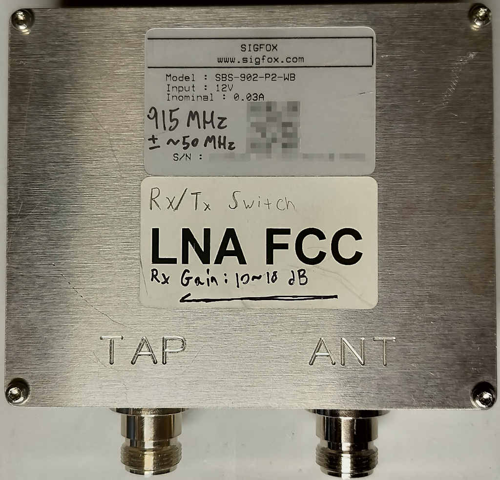
This device is pretty simple on the outside, just two N connectors. The one labeled “ANT” goes to the antenna, and the one labeled “TAP” goes back to the base station and provides power to the LNA. The writing on the label is from me a while back when I originally tested it.
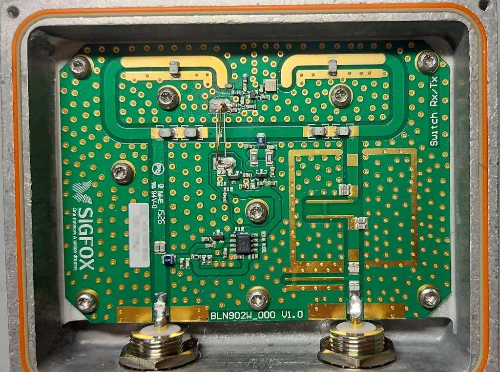
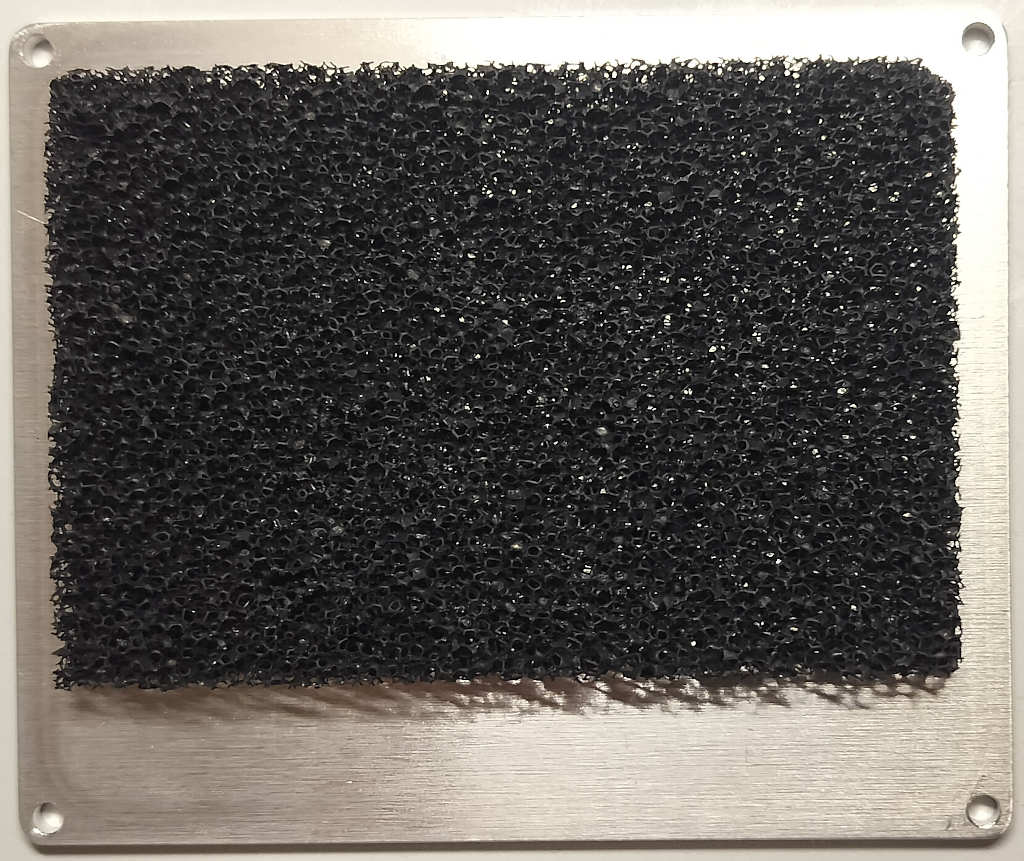
Inside the enclosure we find the PCB, which is relatively simple save for some of the RF structures. Underneath the cover there is also a somewhat conductive foam material, possibly to reduce the potential for resonance.
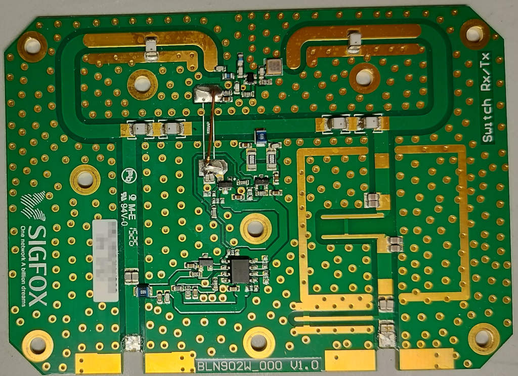
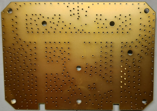
The PCB in this case is really only one layer, the bottom layer is 100% ground plane. This makes it pretty easy to follow where everything is going.
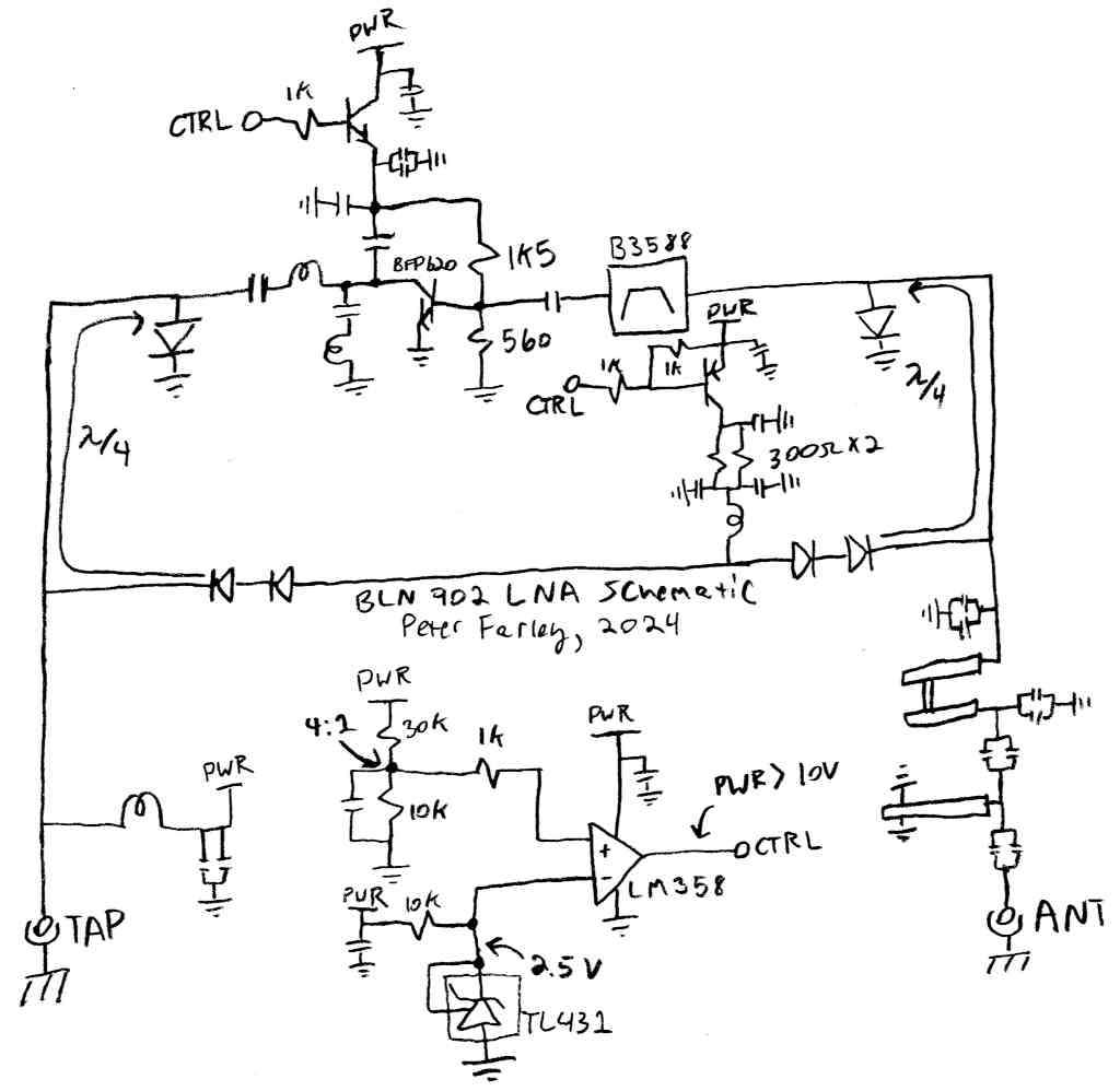
As with the power amplifier, I made a full schematic for the LNA. This one is also pretty simple (much simpler, in fact), so there is not a lot to go over. As a result, I didn’t feel it was worth it to create a block diagram this time.
Power and control
At the TAP port, we find a bias tee (this may not be the correct term, it’s doing the reverse of what you would typically call a bias tee - it’s stripping off the DC, and letting the AC pass onwards) that taps off the DC voltage from the signal to power the amplifier and switching circuitry.
The label on the device states that the input voltage should be 12 V. However, this is only the case when the device is in Rx mode. You would not want the transmit signal appearing at the output of the LNA, as that would likely damage the amplifier, or at the very least it would cause unwanted reflections. To control this switching, the input DC voltage will actually change depending on what state the base station is in. When in receive mode the supplied voltage will be about 12 V, but when in transmit mode this will be lower, something less than 10 V.
To do the threshold detection, there is a LM358 opamp that is being used as a comparator. The inverting input is connected to a TL431 precision voltage reference that provides a 2.5 V reference voltage. The non-inverting input is connected to the DC rail via a 4:1 resistive divider. Thus, when the input voltage is above about 10 V the LM358’s output is high, and when it’s below 10 V the output is low.
This output in turn controls two things. Firstly, when it is high it turns on an NPN transistor to supply power to the Rx amplifier. Secondly, when it is low, it turns on a PNP transistor to apply a bias to the bypass path. This uses the same PIN-diode and quarter-wave impedance transformer based T/R switch that we saw in the power amplifier, only this time with two diodes in series on each side of the bypass. My guess is that the extra diode is used to make the voltage drop closer to the input voltage, so the resistors and transistor don’t need to pass as much current, though I’m not certain this is the purpose.
RF path
After the antenna input, there are two distributed-element filters. I don’t really have experience with these sorts of microstrip designs, and could not find any examples of these two filter styles online, so instead I (roughly) modeled and simulated then in QucsStudio:
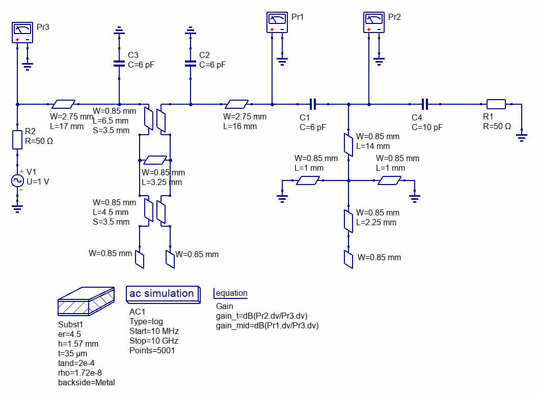
This isn’t the most accurate model, but I just wanted to get a rough idea so I didn’t spend too much time on it.
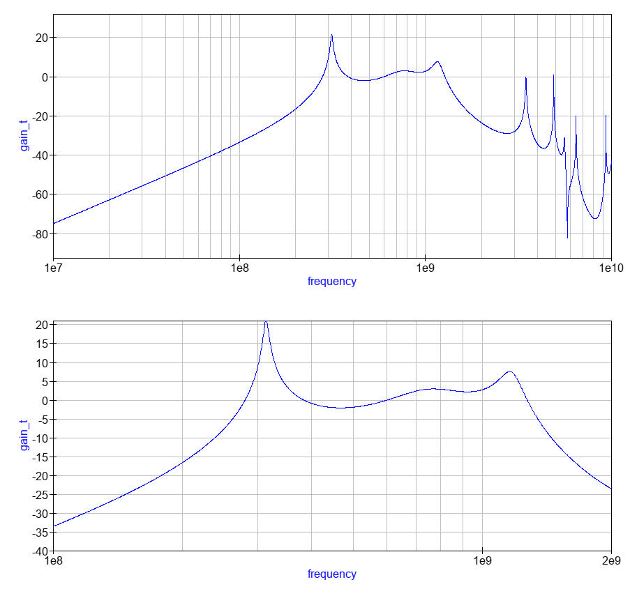
The simulated filter is a fairly broad band-pass filter, from approximately 250-1500 MHz. Given my real-world tests (which I will go over later), I think there is some error in my model, as it should likely be closer to 650-1000 MHz (when in transmit/bypass mode). Though it is also possible that other portions of the PCB are also acting as filters, particularly the T/R switches. Either way - I trust the simulation enough to say that these are acting as a band-pass filter, but not enough to make any assertions as to its stop frequencies.
After the filters, it then goes through the first T/R switch, then through another filter. This is a B3588, the same 915 MHz SAW filter as we saw on the input of the power amplifier. After that, it is amplified by a BFP620 - this was also used as the receive amplifier in the power amplifier. After that, it goes through the second T/R switch and out to the base station.
The TX path bypasses everything except for the two distributed-element filters.
Testing
I was curious as to the actual performance (gain and bandwidth) of the LNA, so I did some testing with a spectrum analyzer.
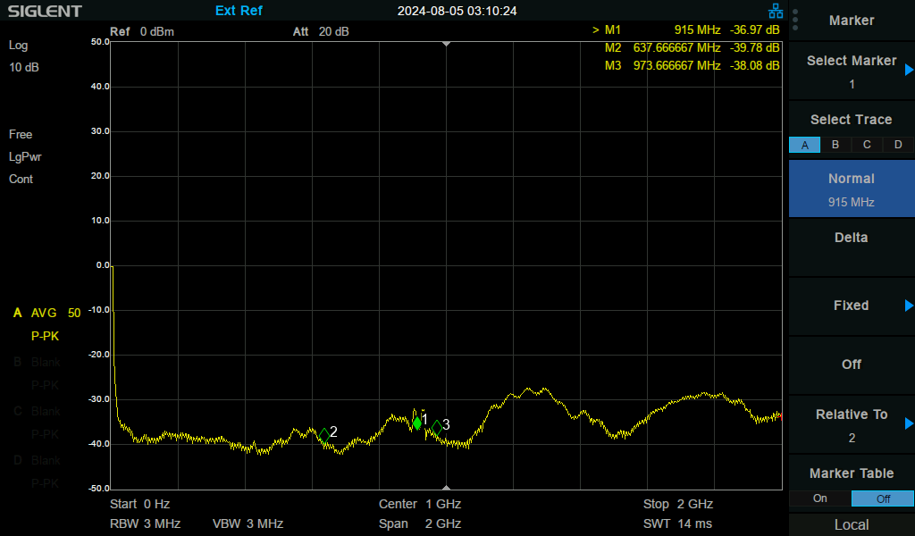
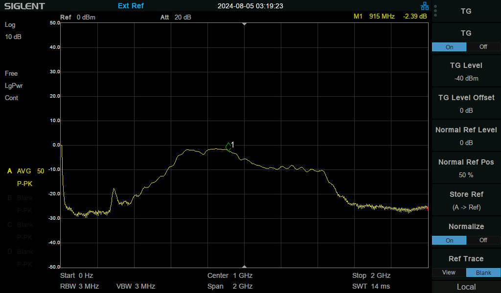
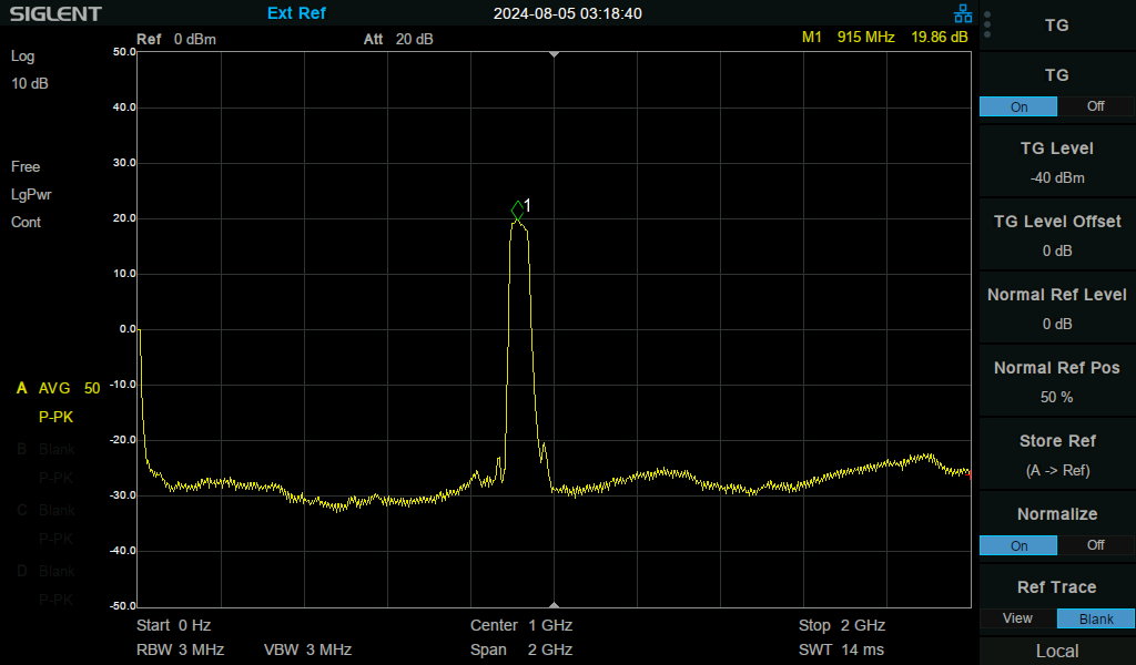
TX path

When the LNA is receiving no DC voltage, effectively no signal gets through, though at around 915 MHz it is only attenuated by about 25 dB, likely leaking through the Rx amplifier.
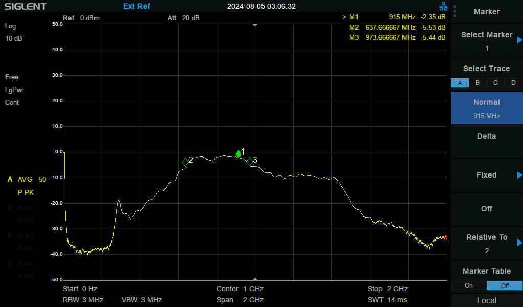
When the LNA is receiving enough voltage to activate the bypass, but still below 10 V so it doesn’t switch to receive mode, the unit effectively acts as a band-pass filter from about 650 to 1000 MHz (with only 10 dB of attenuation until around 1400 MHz).
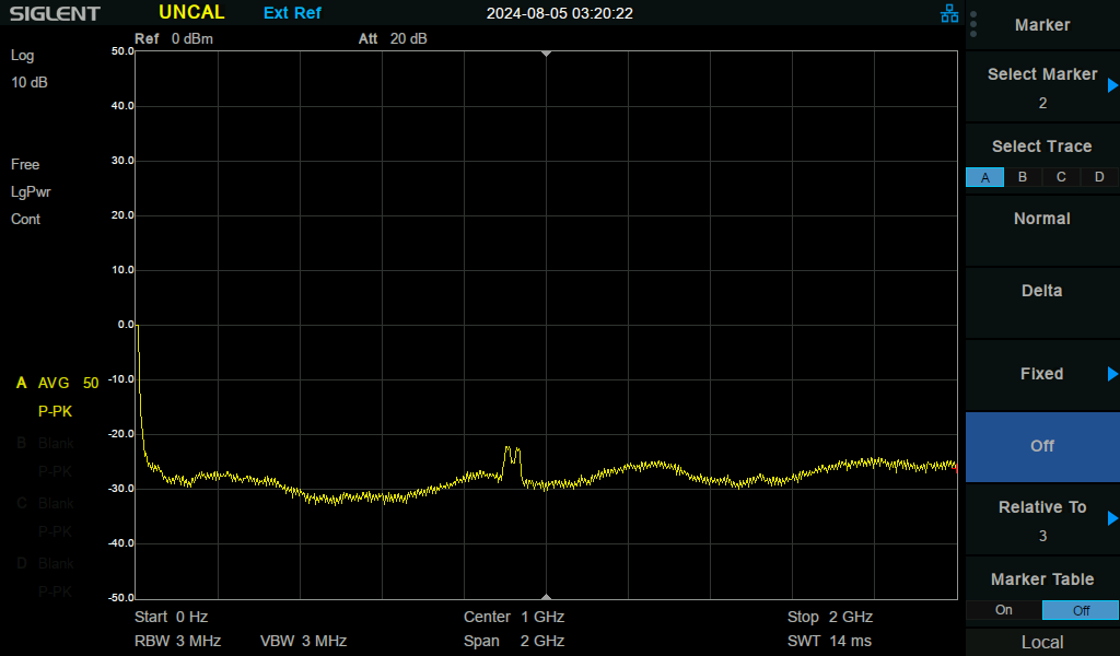
When the LNA is switched to receive mode, a small amount of signal from the TAP port can leak to the ANT port, but it is attenuated by about 30~40 dB. Some sharper points can be seen around the 915 MHz band (the marker is sort of in the way, but I can’t be bothered to set up the test again), where it is likely leaking through the Rx amplifier. Obviously in actual operation, this situation should not occur.
RX path
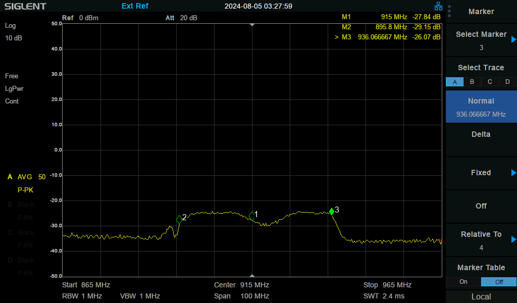
When the LNA is unpowered, the signal is heavily attenuated, though a little signal about 915 MHz leaks through the amplifier.
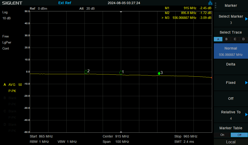
At 9 V, Rx is acting more-or-less the same as Tx, as it simply flows through the bypass path.
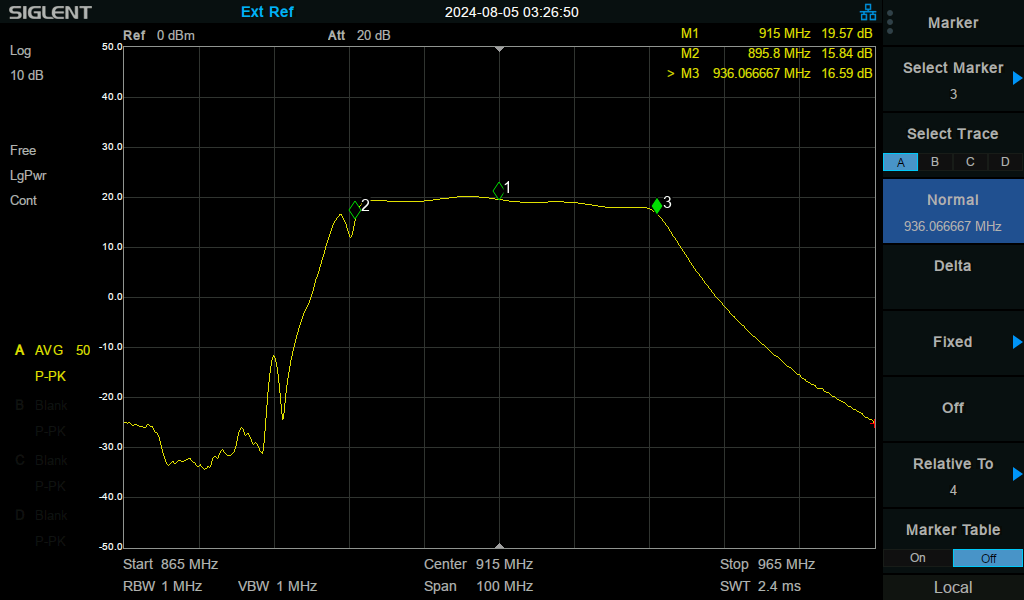
At 12 V, we see a very prominent amplification of the signal around 915 MHz by about 20 dB (at least with an input power of ~-40 dBm), with a bandwidth of about 40 MHz, or maybe 50 MHz if you ignore the dip at around 890 MHz.
Now that we’ve taken a look at the power amplifier and the LNA, the last major component will be the SDR (I may also choose to take a more in-depth look at the power supply and control board, but that would come after if so). That will be much more complex than the previous two. It’s (at least) a 4-layer board, and has quite a lot more going on, so I will likely stick to more of a block-diagram level rather than attempting to recreate the full schematic.