Sigfox Base Station Reverse Engineering - Part 4: SDR
Finally I’ve come to the most complex part of the Sigfox (ignoring the standard PC motherboard) - the SDR (Software Defined Radio). I had originally intended to only get a high-level block diagram of this part, but I ended up going a lot deeper than I planned, and have a good amount of it reverse-engineered. I left out a lot of the power circuitry, and there are some parts I didn’t bother tracing due to it being a 4-layer board (and manual probing is quite time consuming), but apart from that a lot of the blocks are complete (the circuitry within a block was relatively simple to map out, but between blocks was more difficult). Due to the amount of time I spend looking at this, and having been busy lately (I’ve had most of the reverse-engineering complete for about a month now, but haven’t worked on it since), I kind of just want to get this out without spending too much time on it, plus I was sick while finishing and reviewing this, so it might be a little more half-assed than the previous posts
High-level overview
As this one is a lot more complicated than the previous components, I split the schematic up for each block, otherwise it would be quite a mess and unreadable.
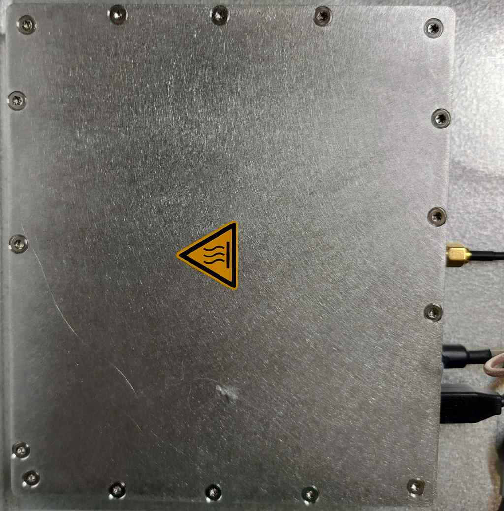
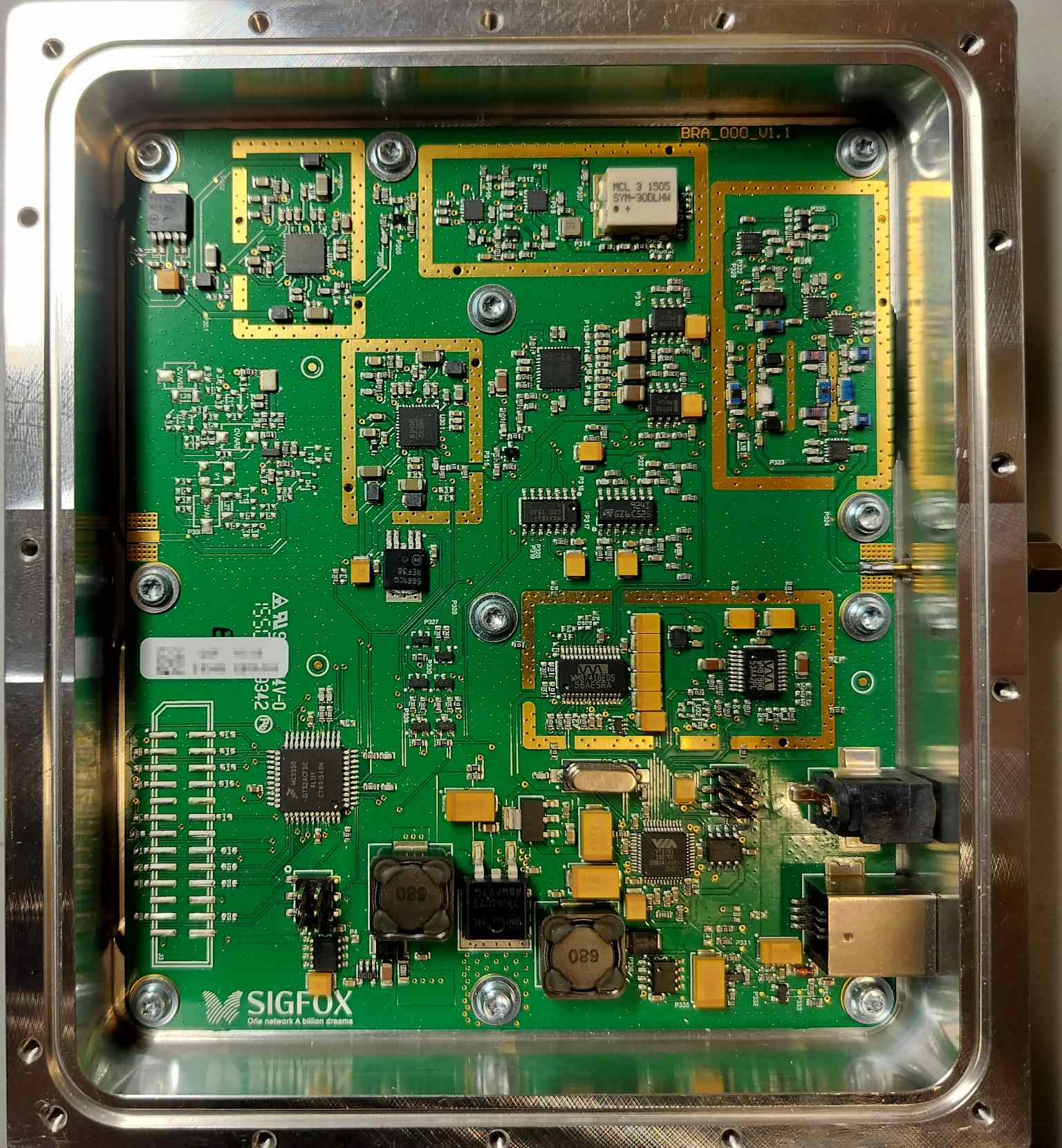
The SDR is enclosed in a machined aluminum chassis. There was a RF gasket in the channel visible in the second image, but I left that with the main base station as it easily falls out. The top lid (as seen installed in the first image) is screwed down securely to create an RF seal. To my eyes the screws seem pretty haphazardly-placed, especially the two right next to each-other in the corner, but perhaps there is reasoning behind their placement.
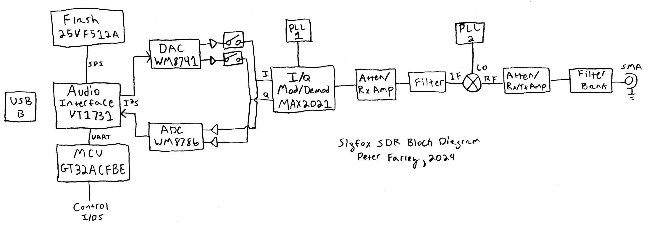
To start with, here is the block diagram that gives a high-level overview of the SDR. The communication between it and the host embedded PC is done completely over USB (this is great, since it means it can possibly be used standalone - more on this later). The audio interface handles all the USB communication, and much of the I/O (for controlling the various blocks) is handled by a microcontroller connected via a UART to the audio interface. The audio interface is in turn connected to both a DAC and an ADC
For the Tx path, the output of the DAC is fed into an amplifier, followed by an analog switch, then finally the I/Q (de)modulator. The output of this then goes through a selectable attenuator (and Rx gain), a filter, then a mixer to reach the target RF frequency. This then goes through another selectable attenuator/gain block, a selectable filter block, and finally exits through the SMA connector. The Rx path is the same just in reverse - except that at the output (I/Q components) of the I/Q (de)modulator it goes to the ADC via an amplifier.
Audio interface, DAC, and ADC
The audio interface being used is a VIA VT1731. There is very little information on this chip available online, even though it does appear to have been used in several consumer products. It seems that VIA does not like to make the documentation public, so presumably users of the chip would need to request it under NDA.
The part is no longer listed on their site, but I was able to find a brief spec sheet via the Internet Archive. This states that it supports sample rates up to 384 kHz, and sample resolution of up to 32-bit, so seemingly a pretty high-end audio part. It also has a 8032 core (related to the Intel 8051 MCU family), with support for UART, I2C, and SPI. The code for the 8032 core is stored on an adjacent 25VF512A 512 Kb SPI flash chip. I was able to dump this, and confirmed the existence of 8051-compatible instructions via Ghidra. I might go further into the reverse-engineering of this code in the future, but it would probably be easier to just work with the drivers on the PC-side, since much of that is just written in plain Python that I can read without disassembling (though there is also a custom Linux driver that does the direct interfacing with the SDR). The chip is usable as an audio interface under Linux, but it won’t have any support for the control of the SDR out of the box.
The ADC is a Wolfson (now Cirrus Logic) WM8786, and the DAC is a WM8741. These are both 24-bit 192 kHz devices (the DAC supports 32-bit input, but it is reduced to 24-bit internally). The inputs/outputs of these chips are differential.
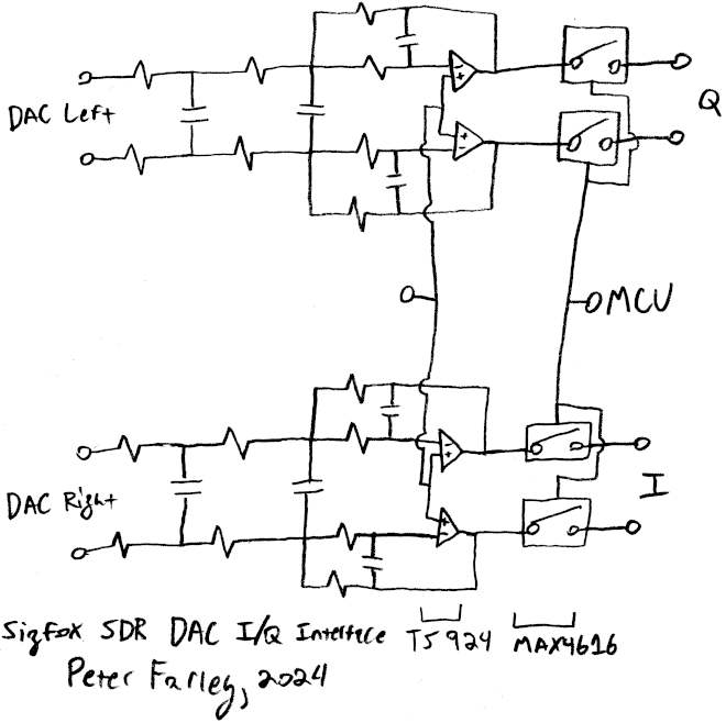
The outputs of the DAC are fed into fully differential amplifiers made up of TS924 opamps, then through a MAX4616 analog switch (to prevent interfering with Rx) to the I/Q (de)modulator.
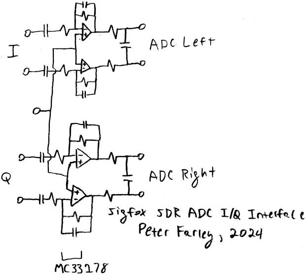
The ADC is fed from the I/Q (de)modulator through a similar pair of fully differential amplifiers, though built using a pair of MC33178 opamps.
Microcontroller
To handle the control of the various components apart from the audio interface, the board uses a Freescale (now NXP) MC9S08GT32A MCU. It handles control of various aspects of the SDR, including the PLLs, some of the LDOs, the selectable gain, attenuation, and filter blocks, and the I/Q (de)modulator.
These chips use the Background Debug Mode (BDM) interface to enable debugging, and I was hopeful that I would be able to dump its firmware. Since I don’t have any hardware that supports the BDM interface, I wrote a basic BDM dumper for the Glasgow Interface Explorer. While I was able to successfully communicate with the chip, it appears that they did lock this device, so unfortunately I wasn’t able to extract the firmware. Not that it would have done me much good anyway, as it would still be up to the VT1731 to actually control it, unless I made some modifications to the board.
I/Q (de)modulator
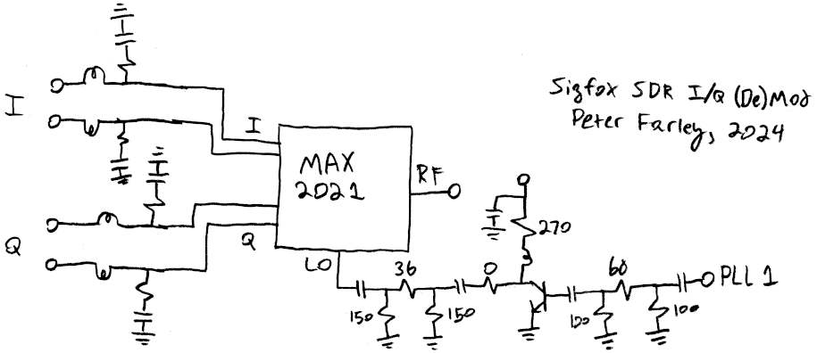
The core of this SDR, apart from the audio interface, is the I/Q (de)modulator - a Maxim Integrated (now a part of Analog Devices) MAX2021. It is rated for direct operation between 650 to 1200 MHz.
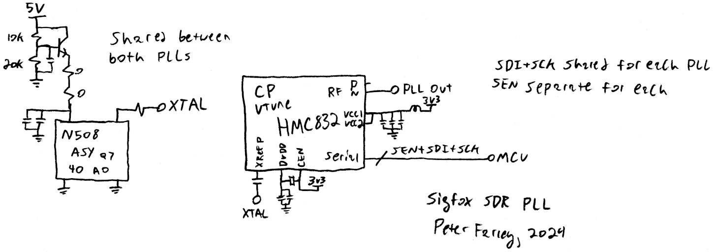
The LO for the MAX2021 is provided by a Analog Devices HMC832 PLL. Both this and the second PLL share the same 40 MHz oscillator. I’m not sure what frequency they are operating the MAX2021 at though, since the second PLL feeds a mixer later in the chain - they may be fixing this stage at a single frequency, and using the mixer to select the operating frequency. Perhaps the MAX2021 doesn’t handle changes in frequency quickly/cleanly enough for the requirements of the Sigfox protocol (pure speculation). Once I have the SDR actually working, I will probably investigate this further.
Amplification/attenuation and mixer

At the RF port of the MAX2021 there is a selectable attenuation and Rx gain block, a filter, and a mixer. The attenuation/gain block is composed of two Peregrine Semiconductor (now part of Murata) PE42641 SP4T RF switches (controlled by the MCU), with different signal paths in-between:
- ~10 dB attenuator (assuming 50 ohms)
- Single capacitor
- Not connected
- BFP620-based Rx amplifier
After this comes a filter, though I was not able to find any information on it.
It has markings 698 530S, presumably some form of SAW bandpass filter.
Following this is a Mini-Circuits SYM-30DLHW mixer, with the LO fed by another
HMC832 PLL.
Input/Output

Finally after the mixer comes two more blocks with selectable paths using two PE42641 each - also controlled by the MCU.
Gain/attenuation selection:
- ~10 dB attenuator (assuming 50 ohms)
- Direct connection
- GVA-84+-based Tx amplifier
- BFP620-based Rx amplifier
Filter selection: this has four different filter paths, seemingly different band-pass filters. Without knowing all the component values (I don’t have time for that) or removing components and testing, it is hard to say what bands these are selecting.
The other end of this filter selector goes to the SMA connector on the enclosure for the SDR, which would in turn route to the Tx Power Amplifier and then to the N connector on the chassis of the base station that will lead to the antenna.
Power
The SDR has a barrel jack for its main power input, taking 9 V. This is then regulated to 5 and 3.3 V for different components. There are at least 6 separate regulators on the board, most being linear regulators but one being a switching buck regulator, with more-or-less each major component (apart from the RF blocks between the MAX2021 and the SMA connector) having their own regulator. This is likely in order to reduce noise from any one component from impacting another, and the board also has a considerable number of decoupling capacitors to this same end.
Assuming there is negligible current consumed from the 5 V USB input, the device draws about 700 mA with just the 9 V connected, and about 880 mA when plugged in to a USB host. This is with the board sitting idle, presumably there would be some increase in current draw when actively transmitting or receiving.
Future work
This was the last major component of the Sigfox base station. I may take a look at the power supply and I/O board at some point if needed, but I can probably get away with just looking at the code on the PC side to learn how that is controlled.
My next plan is to look into how to actually utilize this SDR for my own purposes - that could include further reverse-engineering of the VT1731, looking at the Python code (and potentially Linux drivers) on the PC side, or both. I plan on making another post when I get something working, but who knows when that will be.